- History & Society
- Science & Tech
- Biographies
- Animals & Nature
- Geography & Travel
- Arts & Culture
- Games & Quizzes
- On This Day
- One Good Fact
- New Articles
- Lifestyles & Social Issues
- Philosophy & Religion
- Politics, Law & Government
- World History
- Health & Medicine
- Browse Biographies
- Birds, Reptiles & Other Vertebrates
- Bugs, Mollusks & Other Invertebrates
- Environment
- Fossils & Geologic Time
- Entertainment & Pop Culture
- Sports & Recreation
- Visual Arts
- Demystified
- Image Galleries
- Infographics
- Top Questions
- Britannica Kids
- Saving Earth
- Space Next 50
- Student Center

- Why does physics work in SI units?
- Is mathematics a physical science?


photoconductivity
Our editors will review what you’ve submitted and determine whether to revise the article.
photoconductivity , the increase in the electrical conductivity of certain materials when they are exposed to light of sufficient energy. Photoconductivity serves as a tool to understand the internal processes in these materials, and it is also widely used to detect the presence of light and measure its intensity in light-sensitive devices.
Certain crystalline semiconductors , such as silicon , germanium , lead sulfide, and cadmium sulfide, and the related semimetal selenium , are strongly photoconductive. Normally, semiconductors are relatively poor electrical conductors because they have only a small number of electrons that are free to move under a voltage. Most of the electrons are bound to their atomic lattice in the set of energy states called the valence band. But if external energy is provided, some electrons are raised to the conduction band, where they can move and carry current. Photoconductivity ensues when the material is bombarded with photons of sufficient energy to raise electrons across the band gap , a forbidden region between the valence and conduction bands. In cadmium sulfide this energy is 2.42 electron volts (eV), corresponding to a photon of wavelength 512 nanometres (1 nm = 10 −9 metre), which is visible green light. In lead sulfide the gap energy is 0.41 eV, making this material sensitive to infrared light.

Because the current ceases when the light is removed, photoconductive materials form the basis of light-controlled electrical switches. These materials are also used to detect infrared radiation in military applications such as guiding missiles to heat-producing targets. Photoconductivity has broad commercial application in the process of photocopying , or xerography , which originally used selenium but now relies on photoconductive polymers . See also photoelectric effect .
Photoconductivity in Materials Research
- Reference work entry
- Cite this reference work entry

- Monica Brinza Ph.D. 3 ,
- Jan Willekens Physics Tutor 4 ,
- Mohammed Benkhedir M.Sc. 5 &
- Guy Adriaenssens Ph.D. 6
Part of the book series: Springer Handbooks ((SHB))
14k Accesses
1 Citations
Photoconductivity is the incremental change in the electrical conductivity of a substance upon illumination. Photoconductivity is especially apparent for semiconductors and insulators, which have low conductivity in the dark. Significant information can be derived on the distribution of electronic states in the material and on carrier generation and recombination processes from the dependence of the photoconductivity on factors such as the exciting photon energy, the intensity of the illumination or the ambient temperature. These results can in turn be used to investigate optical absorption coefficients or concentrations and distributions of defects in the material. Methods involving either steady state currents under constant illumination or transient methods involving pulsed excitation can be used to study the electronic density of states as well as the recombination. The transient time-of-flight technique also allows carrier drift mobilities to be determined.
This is a preview of subscription content, log in via an institution to check access.
Access this chapter
Subscribe and save.
- Get 10 units per month
- Download Article/Chapter or eBook
- 1 Unit = 1 Article or 1 Chapter
- Cancel anytime
- Available as PDF
- Read on any device
- Instant download
- Own it forever
- Available as EPUB and PDF
Tax calculation will be finalised at checkout
Purchases are for personal use only
Institutional subscriptions
Photocurrent as a multiphysics diagnostic of quantum materials

An Introduction to Steady-State and Time-Resolved Photoluminescence
Abbreviations.
alternating current
conduction band
constant-photocurrent method
chemical vapor deposition
dual-beam photoconductivity
density of states
interrupted field time-of-flight
modulated photoconductivity
steady-state photoconductivity
time of flight
transient photoconductivity
R. H. Bube: Photoconductivity of Solids (Wiley, New York 1960)
Google Scholar
R. H. Bube: Photoelectronic Properties of Semiconductors (Cambridge Univ. Press, Cambridge 1992)
S. M. Ryvkin: Photoelectric Effects in Semiconductors (Consultants Bureau, New York 1964)
A. Rose: Concepts in Photoconductivity and Allied Problems (Krieger, Huntington 1978)
S. H. You, K. J. Hong, T. S. Jeong, C. J. Youn, J. S. Park, D. C. Shin, J. D. Moon: J. Appl. Phys. 95 , 4042 (2004)
Article CAS Google Scholar
M. Nesládek, L. M. Stals, A. Stesmans, K. Iakoubovskii, G. J. Adriaenssens, J. Rosa, M. Vaněček: Appl. Phys. Lett. 72 , 3306 (1998)
Article Google Scholar
G. J. Adriaenssens: Philos. Mag. B 62 , 79 (1990) and references therein
C. Main, A. E. Owen: In: Electronic and Structural Properties of Amorphous Semiconductors , ed. by P. G. Le Comber, J. Mort (Academic, London 1973) p. 527
J. G. Simmons, G. W. Taylor: J. Phys. C 7 , 3051 (1974)
G. J. Adriaenssens, N. Qamhieh: J. Mater. Sci. Mater. El. 14 , 605 (2003)
H. Fritzsche, B.-G. Yoon, D.-Z. Chi, M. Q. Tran: J. Non-Cryst. Solids 141 , 123 (1992)
M. Vaněček, J. Kočka, A. Poruba, A. Fejfar: J. Appl. Phys. 78 , 6203 (1995)
M. Vaněček, J. Kočka, J. Stuchlík, A. Tříska: Solid State Commun. 39 , 1199 (1981)
C. Main, S. Reynolds, I. Zrinščak, A. Merazga: Mater. Res. Soc. Symp. Proc. 808 , 103 (2004)
CAS Google Scholar
M. Günes, C. Wronski, T. J. McMahon: J. Appl. Phys. 76 , 2260 (1994)
C. Longeaud, D. Roy, O. Saadane: Phys. Rev. B 65 , 85206 (2002)
H. Oheda: J. Appl. Phys. 52 , 6693 (1981)
R. Brüggemann, C. Main, J. Berkin, S. Reynolds: Philos. Mag. B 62 , 29 (1990)
M. S. Iovu, I. A. Vasiliev, E. P. Colomeico, E. V. Emelianova, V. I. Arkhipov, G. J. Adriaenssens: J. Phys. Condens. Mat. 16 , 2949 (2004)
A. I. Rudenko, V. I. Arkhipov: Philos. Mag. B 45 , 209 (1982)
C. Main, R. Brüggemann, D. P. Webb, S. Reynolds: Solid State Commun. 83 , 401 (1992)
C. Main: J. Non-Cryst. Solids 299 , 525 (2002)
D. Hertel, A. Ochse, V. I. Arkhipov, H. Bässler: J. Imag. Sci. Technol. 43 , 220 (1999)
W. E. Spear: J. Non-Cryst. Solids 1 , 197 (1969)
M. Brinza, E. V. Emelianova, G. J. Adriaenssens: Phys. Rev. B 71 , 115209 (2005)
S. Kasap, B. Polishuk, D. Dodds, S. Yannacopoulos: J. Non-Cryst. Solids 114 , 106 (1989)
G. F. Seynhaeve, R. P. Barclay, G. J. Adriaenssens, J. M. Marshall: Phys. Rev. B 39 , 10196 (1989)
S. Kasap, B. Polishuk, D. Dodds: Rev. Sci. Instrum. 61 , 2080 (1990)
S. Kasap, B. Fogal, M. Z. Kabir, R. E. Johanson, S. K. OʼLeary: Appl. Phys. Lett. 84 , 1991 (2004)
C. Haugen, S. O. Kasap: Philos. Mag. B 71 , 91 (1995)
Download references
Author information
Authors and affiliations.
Laboratorium voor Halfgeleiderfysica, University of Leuven, Celestijnenlaan 200D, B-3001, Leuven, Belgium
Monica Brinza Ph.D.
Jan Willekens Physics Tutor
Mohammed Benkhedir M.Sc.
Guy Adriaenssens Ph.D.
You can also search for this author in PubMed Google Scholar
Corresponding authors
Correspondence to Monica Brinza Ph.D. , Jan Willekens Physics Tutor , Mohammed Benkhedir M.Sc. or Guy Adriaenssens Ph.D. .
Editor information
Editors and affiliations.
Department of Electrical Engineering, University of Saskatchewan, 57 Campus Drive, S7N 5A9, Saskatoon, SK, Canada
Safa Kasap Prof.
Materials Team Leader, SELEX Sensors and Airborne Systems Infrared Ltd., Millbrook Industrial Estate, PO Box 217, SO15 0EG, Southampton, Hampshire, UK
Peter Capper Dr.
Rights and permissions
Reprints and permissions
Copyright information
© 2006 Springer-Verlag
About this entry
Cite this entry.
Brinza, M., Willekens, J., Benkhedir, M., Adriaenssens, G. (2006). Photoconductivity in Materials Research. In: Kasap, S., Capper, P. (eds) Springer Handbook of Electronic and Photonic Materials. Springer Handbooks. Springer, Boston, MA. https://doi.org/10.1007/978-0-387-29185-7_7
Download citation
DOI : https://doi.org/10.1007/978-0-387-29185-7_7
Publisher Name : Springer, Boston, MA
Print ISBN : 978-0-387-26059-4
Online ISBN : 978-0-387-29185-7
eBook Packages : Chemistry and Materials Science Reference Module Physical and Materials Science Reference Module Chemistry, Materials and Physics
Share this entry
Anyone you share the following link with will be able to read this content:
Sorry, a shareable link is not currently available for this article.
Provided by the Springer Nature SharedIt content-sharing initiative
- Publish with us
Policies and ethics
- Find a journal
- Track your research
Thank you for visiting nature.com. You are using a browser version with limited support for CSS. To obtain the best experience, we recommend you use a more up to date browser (or turn off compatibility mode in Internet Explorer). In the meantime, to ensure continued support, we are displaying the site without styles and JavaScript.
- View all journals
- Explore content
- About the journal
- Publish with us
- Sign up for alerts
- Published: 21 September 2023
Ultra-broadband photoconductivity in twisted graphene heterostructures with large responsivity
- H. Agarwal ORCID: orcid.org/0000-0002-9418-7966 1 na1 ,
- K. Nowakowski ORCID: orcid.org/0000-0002-4598-9831 1 na1 ,
- A. Forrer 2 ,
- A. Principi 3 ,
- R. Bertini ORCID: orcid.org/0000-0001-7225-0277 1 ,
- S. Batlle-Porro ORCID: orcid.org/0000-0001-9663-8268 1 ,
- A. Reserbat-Plantey ORCID: orcid.org/0000-0002-9106-8750 1 , 4 ,
- P. Prasad 1 ,
- L. Vistoli 1 ,
- K. Watanabe ORCID: orcid.org/0000-0003-3701-8119 5 ,
- T. Taniguchi ORCID: orcid.org/0000-0002-1467-3105 6 ,
- A. Bachtold 1 , 7 ,
- G. Scalari ORCID: orcid.org/0000-0003-4028-803X 2 ,
- R. Krishna Kumar ORCID: orcid.org/0000-0003-0857-4466 1 &
- F. H. L. Koppens ORCID: orcid.org/0000-0001-9764-6120 1 , 7
Nature Photonics volume 17 , pages 1047–1053 ( 2023 ) Cite this article
5911 Accesses
12 Citations
29 Altmetric
Metrics details
- Optical properties and devices
- Photonic devices
The requirements for broadband photodetection are becoming exceedingly demanding in hyperspectral imaging. While intrinsic photoconductor arrays based on mercury cadmium telluride represent the most sensitive and suitable technology, their optical spectrum imposes a narrow spectral range with a sharp absorption edge that cuts their operation to <25 μm. Here we demonstrate a large ultra-broadband photoconductivity in twisted double bilayer graphene heterostructures spanning the spectral range of 2–100 μm with internal quantum efficiencies of approximately 40% at speeds of 100 kHz. The large response originates from unique properties of twist-decoupled heterostructures including pristine, crystal field-induced terahertz band gaps, parallel photoactive channels and strong photoconductivity enhancements caused by interlayer screening of electronic interactions by respective layers acting as sub-atomic spaced proximity screening gates. Our work demonstrates a rare instance of an intrinsic infrared–terahertz photoconductor that is complementary metal-oxide-semiconductor compatible and array integratable, and introduces twist-decoupled graphene heterostructures as a viable route for engineering gapped graphene photodetectors with three-dimensional scalability.
This is a preview of subscription content, access via your institution
Access options
Access Nature and 54 other Nature Portfolio journals
Get Nature+, our best-value online-access subscription
24,99 € / 30 days
cancel any time
Subscribe to this journal
Receive 12 print issues and online access
195,33 € per year
only 16,28 € per issue
Buy this article
- Purchase on SpringerLink
- Instant access to full article PDF
Prices may be subject to local taxes which are calculated during checkout

Plasmonic antenna coupling to hyperbolic phonon-polaritons for sensitive and fast mid-infrared photodetection with graphene

Intelligent infrared sensing enabled by tunable moiré quantum geometry

Synergistic-potential engineering enables high-efficiency graphene photodetectors for near- to mid-infrared light
Data availability.
The data that support the plots within this paper and other findings of this study are available from the corresponding authors upon reasonable request.
Code availability
All codes used to produce the findings of this study are available from the corresponding authors on reasonable request.
Richards, P. L. & McCreight, C. R. Infrared detectors for astrophysics. Phys. Today 58 , 41–47 (2005).
Article Google Scholar
Rieke, G. H. Infrared detector arrays for astronomy. Annu. Rev. Astron. Astrophys. 45 , 77–115 (2007).
Article ADS Google Scholar
Mak, K. F. et al. Measurement of the optical conductivity of graphene. Phys. Rev. Lett. 101 , 196405 (2008).
Gabor, N. M. et al. Hot carrier-assisted intrinsic photoresponse in graphene. Science. 334 , 648–652 (2011).
Yan, J. et al. Dual-gated bilayer graphene hot-electron bolometer. Nat. Nanotechnol. 7 , 472–478 (2012).
Deng, B. et al. Strong mid-infrared photoresponse in small-twist-angle bilayer graphene. Nat. Photonics 14 , 549–553 (2020).
El Fatimy, A. et al. Epitaxial graphene quantum dots for high-performance terahertz bolometers. Nat. Nanotechnol. 11 , 335–338 (2016).
Rogalski, A. HgCdTe infrared detector materials: history, status and outlook. Rep. Prog. Phys. 69 , 2267 (2005).
Wang, F. et al. Gate-variable optical transitions in graphene. Science. 320 , 206–209 (2008).
Zhang, Y. et al. Direct observation of a widely tunable bandgap in bilayer graphene. Nature 459 , 820–823 (2009).
Rickhaus, P. et al. Gap opening in twisted double bilayer graphene by crystal fields. Nano Lett. 19 , 8821–8828 (2019).
Wang, L. et al. One-dimensional electrical contact to a two-dimensional material. Science. 342 , 614–617 (2013).
Cao, Y. et al. Superlattice-induced insulating states and valley-protected orbits in twisted bilayer graphene. Phys. Rev. Lett. 117 , 116804 (2016).
Ju, L. et al. Tunable excitons in bilayer graphene. Science. 358 , 907–910 (2017).
Rösch, M. et al. Heterogeneous terahertz quantum cascade lasers exceeding 1.9 THz spectral bandwidth and featuring dual comb operation. Nanophotonics. 7 , 237–242 (2018).
Huang, P. et al. Ultra-long carrier lifetime in neutral graphene–hBN van der Waals heterostructures under mid-infrared illumination. Nat. Commun. 11 , 1–9 (2020).
ADS Google Scholar
Schaller, R. D., Pietryga, J. M. & Klimov, V. I. Carrier multiplication in InAs nanocrystal quantum dots with an onset defined by the energy conservation limit. Nano Lett. 7 , 3469–3476 (2007).
Josh, N. V. Photoconductivitiy Art, Science And Technology (CRC Press, 1990).
Icking, E. et al. Transport spectroscopy of ultraclean tunable band gaps in bilayer graphene. Adv. Electron. Mater. 8 , 2200510 (2022).
Nam, Y., Ki, D. K., Soler-Delgado, D. & Morpurgo, A. F. Electron–hole collision limited transport in charge-neutral bilayer graphene. Nat. Phys. 13 , 1207–1214 (2017).
Tan, C. et al. Dissipation-enabled hydrodynamic conductivity in a tunable bandgap semiconductor. Sci. Adv. 8 , 1–8 (2022).
Kim, M. et al. Control of electron-electron interaction in graphene by proximity screening. Nat. Commun. 11 , 2339 (2020).
Lu, C. P. et al. Local, global, and nonlinear screening in twisted double-layer graphene. Proc. Natl Acad. Sci. USA 113 , 6623–6628 (2016).
Wu, X. et al. Boosting carrier mobility of synthetic few layer graphene on SiO 2 by interlayer rotation and decoupling. Adv. Mater. Interfaces 5 , 1–7 (2018).
Rickhaus, P. et al. The electronic thickness of graphene. Sci. Adv. 6 , eaay8409 (2022).
Ulstrup, S. et al. Ultrafast dynamics of massive Dirac fermions in bilayer graphene. Phys. Rev. Lett. 112 , 257401 (2014).
Huang, M. et al. Large-area single-crystal AB-bilayer and ABA-trilayer graphene grown on a Cu/Ni(111) foil. Nat. Nanotechnol. 15 , 289–295 (2020).
Mannix, A. J. et al. Robotic four-dimensional pixel assembly of van der Waals solids. Nat. Nanotechnol. 17 , 361–366 (2022).
Tomadin, A., Brida, D., Cerullo, G., Ferrari, A. C. & Polini, M. Nonequilibrium dynamics of photoexcited electrons in graphene: collinear scattering, Auger processes, and the impact of screening. Phys. Rev. B 88 , 35430 (2013).
Rogalski, A. Semiconductor detectors and focal plane arrays for far-infrared imaging. Opto-Electronics Rev. 21 , 406–426 (2013).
Kim, K. et al. Tunable moiré bands and strong correlations in small-twist-angle bilayer graphene. Proc. Natl Acad. Sci. USA 114 , 3364–3369 (2017).
Pizzocchero, F. et al. The hot pick-up technique for batch assembly of van der Waals heterostructures. Nat. Commun. 7 , 11894 (2016).
Purdie, D. G. et al. Cleaning interfaces in layered materials heterostructures. Nat. Commun. 9 , 1–12 (2018).
Ferrari, A. C. et al. Raman spectrum of graphene and graphene layers. Phys. Rev. Lett. 97 , 187401 (2006).
Download references
Acknowledgements
We thank D. B. Ruiz, S. Castilla, D. De Fazio, M. Amir Ali, G. Li, A. Berdyugin, M. Polini, V. Mkhitaryan, G. Kumar, and I. Torre for technical discussions. We further thank M. Ceccanti for making the illustration presented in Fig. 1a . H.A., K.N. and R.B. acknowledge funding from the European Union’s Horizon 2020 research and innovation programme under Marie Skłodowska-Curie grant agreement no. 665884, 713729 and 847517, respectively. S.B.-P. acknowledges funding from the Presidencia de la Agencia Estatal de Investigación within the PRE2020-094404 predoctoral fellowship. G.S. and A.F. gratefully acknowledge funding from the ERC grant CHIC (no. 724344), and J. Faist for discussions. A.P. acknowledges support from the European Union’s Horizon 2020 research and innovation programme under Marie Sklodowska-Curie grant agreement no. 873028 and from the Leverhulme Trust under grant agreement RPG-2019-363. K.W. and T.T. acknowledge support from the Elemental Strategy Initiative conducted by MEXT Japan with grant no. JPMXP0112101001, JSPS KAKENHI (JP19H05790, JP20H00354 and JP21H05233) and CREST (JPMJCR15F3), JST. R.K.K. acknowledges the EU Horizon 2020 programme under MarieSkłodowska-Curie grants 754510 and 893030 and the FLAG-ERA grant (PhotoTBG, PCI2021-122020-2A), by ICFO, RWTH Aachen and ETHZ/Department of Physics. A.B. acknowledges support from ERC advanced grant no. 692876, MICINN grant no. RTI2018-097953-B-I00 and PID2021-122813OB-I00, AGAUR (grant no. 2017SGR1664), the Fondo Europeo de Desarrollo, the Spanish Ministry of Economy and Competitiveness through Quantum CCAA, EUR2022-134050, and CEX2019-000910-S [MCIN/AEI/10.13039/501100011033], MCIN with funding from European Union NextGenerationEU (PRTR-C17.I1), Fundacio Cellex, Fundacio Mir-Puig, Generalitat de Catalunya through CERCA. F.H.L.K. acknowledges support from the ERC TOPONANOP (726001), Fundació Cellex, Fundació Mir-Puig, Generalitat de Catalunya (CERCA, AGAUR, SGR 1656, program TWIST), the Government of Spain [PID2019-106875GB-I00; PCI2021-122020-2A; PDC2022-133844-I00 (Teracomm); Severo Ochoa CEX2019-000910-S] funded by MCIN/AEI/10.13039/501100011033 and by the European Union NextGenerationEU/PRTR. Furthermore, the research leading to these results has received funding from the European Union’s Horizon 2020 research and innovation programme under grant agreement no. 881603 (Graphene flagship Core3), 820378 (Quantum flagship) and 101034929 (Fastera). This material is based upon work supported by the Air Force Office of Scientific Research under award number FA8655-23-1-7047. Any opinions, findings, and conclusions or recommendations expressed in this material are those of the author(s) and do not necessarily reflect the views of the United States Air Force.
Author information
These authors contributed equally: H. Agarwal, K. Nowakowski.
Authors and Affiliations
Institut de Ciències Fotòniques, The Barcelona Institute of Science and Technology, Castelldefels, Spain
H. Agarwal, K. Nowakowski, R. Bertini, S. Batlle-Porro, A. Reserbat-Plantey, P. Prasad, L. Vistoli, A. Bachtold, R. Krishna Kumar & F. H. L. Koppens
Quantum Optoelectronics Group, Institute of Quantum Electronics, ETH Zürich, Zürich, Switzerland
A. Forrer & G. Scalari
School of Physics and Astronomy, University of Manchester, Manchester, UK
A. Principi
Université Côte d’Azur, CNRS, CRHEA, Valbonne, France
A. Reserbat-Plantey
Research Center for Functional Materials, National Institute for Materials Science, Tsukuba, Japan
K. Watanabe
International Center for Materials Nanoarchitectonics, National Institute for Materials Science, Tsukuba, Japan
T. Taniguchi
Institució Catalana de Recerca i Estudis Avançats, Barcelona, Spain
A. Bachtold & F. H. L. Koppens
You can also search for this author in PubMed Google Scholar
Contributions
F.H.L.K., H.A. and R.K.K. conceived the presented idea. H.A. fabricated the devices. H.A. and K.N. performed the mid-infrared measurements with inputs from R.K.K. and F.H.L.K. K.N. built the mid-infrared measurement setup with inputs from A.R.-P., R.K.K. and F.H.L.K. R.K.K, and H.A. performed terahertz far-field photocurrent measurements A.R.-P, R.K.K. and H.A. designed and built the measurement setup for terahertz photocurrent experiments. A.F., H.A. and G.S. performed low-temperature FTIR spectroscopy measurements. A.P., R.K.K. and F.H.L.K. developed the theoretical formalism and performed the analytical calculations. R.B. performed absorption calculations. K.W. and T.T. provided hBN crystals. H.A, P.P., L.V. and A.B. performed magnetotransport experiments. H.A., K.N. and R.K.K. analysed the results. R.K.K., H.A. and F.H.L.K. wrote the manuscript. R.K.K. and F.H.L.K. supervised the project. All authors provided critical feedback and helped shape the research, analysis and manuscript.
Corresponding authors
Correspondence to R. Krishna Kumar or F. H. L. Koppens .
Ethics declarations
Competing interests.
The authors declare no competing interests.
Peer review
Peer review information.
Nature Photonics thanks the anonymous reviewers for their contribution to the peer review of this work.
Additional information
Publisher’s note Springer Nature remains neutral with regard to jurisdictional claims in published maps and institutional affiliations.
Supplementary information
Supplementary information.
Supplementary Sections 1–9.
Rights and permissions
Springer Nature or its licensor (e.g. a society or other partner) holds exclusive rights to this article under a publishing agreement with the author(s) or other rightsholder(s); author self-archiving of the accepted manuscript version of this article is solely governed by the terms of such publishing agreement and applicable law.
Reprints and permissions
About this article
Cite this article.
Agarwal, H., Nowakowski, K., Forrer, A. et al. Ultra-broadband photoconductivity in twisted graphene heterostructures with large responsivity. Nat. Photon. 17 , 1047–1053 (2023). https://doi.org/10.1038/s41566-023-01291-0
Download citation
Received : 08 March 2023
Accepted : 18 August 2023
Published : 21 September 2023
Issue Date : December 2023
DOI : https://doi.org/10.1038/s41566-023-01291-0
Share this article
Anyone you share the following link with will be able to read this content:
Sorry, a shareable link is not currently available for this article.
Provided by the Springer Nature SharedIt content-sharing initiative
This article is cited by
Enhancing shift current response via virtual multiband transitions.
- Swati Chaudhary
- Cyprian Lewandowski
Communications Physics (2024)
Large-angle twist effect
- Bingchen Deng
- Fengnian Xia
Nature Photonics (2023)
Quick links
- Explore articles by subject
- Guide to authors
- Editorial policies
Sign up for the Nature Briefing newsletter — what matters in science, free to your inbox daily.

- Electrical and Electronics Job Interview Questions and Answers
- Multiple Choice Questions with Answers (MCQs)
- Comparisons in Electrical and Electronics
Photoconductivity – Definition, Working and its Applications:
Photoconductivity – When excess electrons and holes are produced in a semiconductor, there is a corresponding increase in conductivity of a sample as indicated by the following equation
Conductivity of semiconductor,
The above equation is obtained from Eqs. (6.48) and (6.59).
When the excess carriers in a semiconductor are due to optical luminescence, the resulting conductivity is called photoconductivity . This is an important effect, with useful applications in the analysis of semiconductor materials and in the operation of different types of devices.
The photoconductive effect is explained as follows:
The conductivity of a material is proportional to the concentration of charge carriers present, as indicated by Eq. (25.10). Radiant energy supplied to the semiconductor causes covalent bonds to the broken, and EHPs in excess of those generated thermally are produced. These increased current carriers reduce the resistance of the material and, therefore, such a device is called a photoconductor or photoresistor .

Energy diagram of a semiconductor having both acceptor and donor impurities is given in Fig. 25.10. When this specimen is illuminated by photons of sufficient energies, the possible transitions are as follows :
An EHP can be generated by a high-energy photon, in what is called intrinsic excitation ; a photon may excite a donor electron into the conduction band ; or a valence electron may move into an acceptor state. The last two transitions are called the impurity excitations . Since the density of states in the conduction and valence bands greatly exceeds the density of impurity states, photoconductivity is due principally to intrinsic excitation.
Spectral Response: The minimum energy of a photon required for intrinsic excitation is the forbidden-gap energy E G , in electron volts, of the semiconductor material. The long-wavelength threshold of the material is defined as the wavelength corresponding to the energy gap E G and is given by Eq. (25.11)
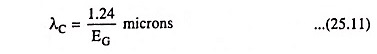
For silicon, E G = 1.1 eV and λ C = 1.13 microns
whereas for germanium, E G = 0.72 eV and λ C = 1.73 microns at room temperature.

The spectral-sensitivity curves for silicon and germanium are given in Fig. 25.11. The worth noting point is that the long-wavelength limit is slightly greater than the calculated values of λ C . This is due to impurity excitations. With the decrease of the wavelength, the response increases and attains a maximum value.
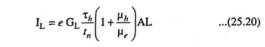
Photoconductive Current: The carriers generated by photoexcitation will move under the influence of an applied field, If they survive recombination, they will reach ohmic contacts at the ends of the semiconductor bar, and thus the device current will be constituted. The current may be given by
where G L is the generation rate of excess carriers, in cm -3 s -1 , produced by optical luminescence, τ is the average life time of the newly generated carriers and t t is the average transit time for carriers to reach the ohmic contacts.
Photoconductor:

Figure 25.12 depicts a semiconductor bar with ohmic contacts at each end and a voltage applied between the terminals. The initial thermal-equilibrium conductivity is given by
When the excess carriers are created in the semiconductor, the conductivity becomes
where δn and δp are the excess electron and hole concentrations, respectively. Considering an N-type semiconductor, it can be assumed that δn = δp. Using δp as the concentration of excess carriers, in steady-state, the carrier concentration is given by
where G L is the generation rate of excess carriers and τ h is the lifetime of excess minority carriers.
The conductivity from Eq. (25.14) can be written as
The change in conductivity due to the optical excitation, called a photoconductivity, is then
Applied voltage induces an electric field in the semiconductor and a current is caused by this electric field. The current density is given by
where J 0 is the current density in the semiconductor prior to optical excitation and J L is the photocurrent density. The photocurrent density, J L = ΔσE. In case of uniform generation of excess electrons and holes throughout the semiconductor, photocurrent is given as
where A is the x-sectional area of the semiconductor device. The photocurrent varies directly as the excess carrier generation rate, which in turn is proportional to the incident photo flux .
If excess carriers (electrons and holes) are not generated uniformly throughout the semiconductor material, then the total photocurrent is determined by integrating the photoconductivity over the cross-sectional area.
Since μ e E is the electron drift velocity, the electron transit time (time required for an electron to flow through the photoconductor) is given as

where L is the length of the semiconductor device.
The photocurrent is given, by Eq. (25.18),
Photoconductor gain can be defined as the ratio of the rate at which charge is collected by the contacts to the rate at which charge is created within the photoconductor i.e.

and substituting the value of I L from Eq. (25.20) in Eq. (25.21) we have

Related posts:
- Step up Chopper – Definition, Circuit Diagram and its Working Principle
- Astable Multivibrator Definition and its Working
- Pin Photodiode – Definition, Working and Applications
- Projection Welding – Definition, Working, Advantages and Applications
- Percussion Welding – Definition, Working, Advantages and Applications
- Electric Arc Welding – Definition, Working Principle, Types and Applications
- What is Thyristor? – Thyristor Family and its Applications
- Nuclear Reactor – Definition and its Components
- What is Short Circuit Current? – Definition and its Process
- Photodetectors – Definition and Applications
- Light Dependent Resistors (LDRs) – Definition, Construction, Workings and Applications
- Facsimile (FAX) Machine – Definition, Operation and Applications
- Butt Welding – Definition, Types and Applications
- What is Electrodes? – Definition, Types, Applications and Advantages
- What is Electroforming Process? – Definition and Applications
- Amplidyne (Rotary Amplifier) – Definition, Construction, Connection Diagram, Workings and Applications
- Electromagnetic Attraction Relay – Working Principle and its types
- What is Bleeder Resistor? – Working and Its Functions
- What is Electroplating in Electrolysis and its Working Principle
- Counter Emf Automatic Starter – Working Principle and its Drawbacks
Grab your spot at the free arXiv Accessibility Forum
Help | Advanced Search
Condensed Matter > Materials Science
Title: photoluminescence and high temperature persistent photoconductivity experiments in sno2 nanobelts.
Abstract: The Persistent Photoconductivity (PPC) effect was studied in individual tin oxide (SnO2) nanobelts as a function of temperature, in air, helium, and vacuum atmospheres, and low temperature Photoluminescence measurements were carried out to study the optical transitions and to determine of the acceptor/donors levels and their best representation inside the band gap. Under ultraviolet (UV) illumination and at temperatures in the range of 200 to 400K we observed a fast and strong enhancement of the photoconductivity, and the maximum value of the photocurrent induced increases as the temperature or the oxygen concentration decreases. By turning off the UV illumination the induced photocurrent decays with lifetimes up to several hours. The photoconductivity and the PPC results were explained by adsorption and desorption of molecular oxygen at the surface of the SnO2 nanobelts. Based on the temperature dependence of the PPC decay an activation energy of 230 meV was found, which corresponds to the energy necessary for thermal ionization of free holes from acceptor levels to the valence band, in agreement with the photoluminescence results presented. The molecular-oxygen recombination with holes is the origin of the PPC effect in metal oxide semiconductors, so that, the PPC effect is not related to the oxygen vacancies, as commonly presented in the literature.
| Comments: | 6 pages, 10 figures, submitted to "The Journal of Physical Chemistry C" |
| Subjects: | Materials Science (cond-mat.mtrl-sci); Mesoscale and Nanoscale Physics (cond-mat.mes-hall) |
| Cite as: | [cond-mat.mtrl-sci] |
| (or [cond-mat.mtrl-sci] for this version) | |
| Focus to learn more arXiv-issued DOI via DataCite |
Submission history
Access paper:.
- Other Formats
References & Citations
- Google Scholar
- Semantic Scholar
BibTeX formatted citation
Bibliographic and Citation Tools
Code, data and media associated with this article, recommenders and search tools.
- Institution
arXivLabs: experimental projects with community collaborators
arXivLabs is a framework that allows collaborators to develop and share new arXiv features directly on our website.
Both individuals and organizations that work with arXivLabs have embraced and accepted our values of openness, community, excellence, and user data privacy. arXiv is committed to these values and only works with partners that adhere to them.
Have an idea for a project that will add value for arXiv's community? Learn more about arXivLabs .
- Physical Sciences
- Solid State Physics
- Condensed Matter Physics
- Photoconductivity
Experiments on photoconductivity
- European Journal of Physics 33(3):503-511
- 33(3):503-511
- This person is not on ResearchGate, or hasn't claimed this research yet.
Discover the world's research
- 25+ million members
- 160+ million publication pages
- 2.3+ billion citations
No full-text available
To read the full-text of this research, you can request a copy directly from the author.
- APPL PHYS A-MATER

- J MATER SCI-MATER EL

- INT J PHOTOENERGY

- INT J BIFURCAT CHAOS
- K. L. Joiner

- Zhiwei Zhou

- Almas Z. Shaikh
- Shital D. Satpute
- Janardhan R. Gadde

- U. S. Mbamara
- Yaakov Kraftmakher
- Richard H. Bube
- M. G. C. Peiris
- I. K. Perera
- Paul F. Mullaney

- Recruit researchers
- Join for free
- Login Email Tip: Most researchers use their institutional email address as their ResearchGate login Password Forgot password? Keep me logged in Log in or Continue with Google Welcome back! Please log in. Email · Hint Tip: Most researchers use their institutional email address as their ResearchGate login Password Forgot password? Keep me logged in Log in or Continue with Google No account? Sign up
COMMENTS
Photoconductivity is an optical and electrical phenomenon in which a material becomes more electrically conductive due to the absorption of electromagnetic radiation such as visible light, ultraviolet light, infrared light, or gamma radiation. [1]When light is absorbed by a material such as a semiconductor, the number of free electrons and holes increases, resulting in increased electrical ...
Photoconductivity experiments have been extensively used by numerous researchers to characterize various semiconductor materials. Principles of steady-state and modulated photoconductivity (frequency-resolved photoconductivity) are introduced along with their main features in extracting material characteristics such as the density of states in ...
While most photoconductivity experiments involve monitoring the photocurrent in the external circuit, it is also possible to carry out photoconductivity experiments under open circuit conditions. Thus, in addition to the categories above, we need to introduce two more classifications: (C) Short circuit photoconductivity configuration where the ...
Given the complexity of these processes, use of a range of photoconductivity experiments is often advisable, as is the combination of photoconductivity with complementary techniques such as optical absorption , photoluminescence , dark current activation , charge collection , electron paramagnetic resonance and various pump-probe experiments.
In this classic photoconductivity experiment, the thermoelectric effects are insignificant. Instead, the photovoltaic and a photo-induced bolometric effect dominate the photoresponse.
The combined use of different types of photoconductivity experiments is therefore often advisable, as is the combination of photoconductivity with related experiments such as photoluminescence or charge collection. A wide variety of experimental techniques based on photoconductivity have come into general use over the years.
photoconductivity, the increase in the electrical conductivity of certain materials when they are exposed to light of sufficient energy. Photoconductivity serves as a tool to understand the internal processes in these materials, and it is also widely used to detect the presence of light and measure its intensity in light-sensitive devices ...
The experiments described include several topics: spectral response, photosensitivity, photoconductivity gain, rise and decay time constants, and frequency response to modulated light. Along with general information on photoconductivity, the experiments provide good opportunities for training in optical and electrical measurements.
MITOCW | Tutorial: Photoconductivity [MUSIC PLAYING] PROFESSOR: Hello, everyone. In our last demo, we demonstrated how the electrical conductivity of silicon can be changed by over six orders of magnitude by adding dopants that can increase the number of free or mobile charges in the material. Today, we'll
Explore an authoritative resource with coverage of foundational concepts of photoconductivity and photoconductive materials In Photoconductivity and Photoconductive Materials, Professor Kasap delivers a definitive guide to the basic principles of photoconductivity and a selection of present topical photoconductive materials. Divided into two parts, the set begins with basic concepts and ...
general principles of photoconductivity may be found in the standard monographs by Bube [7.1,2], Ryvkin [7.3] and Rose [7.4]. 7.1 Steady State Photoconductivity Methods 7.1.1 The Basic Single-Beam Experiment The simplest photoconductivity experiment uses a con-stant monochromatic light source to generate equal
Photoconductivity, as a well-known optical and electrical phenomenon in semiconductor, is an effect that the electrical conductivity increases due to the absorption of light radiation ... These phenomena were further confirmed by control experiments conducted on CNT film/CuO granular film hetero-dimensional contacts. These interesting results ...
MIT 2.627 Fundamentals of Photovoltaics, Fall 2011View the complete course: http://ocw.mit.edu/2-627F11Instructor: Joe SullivanThis video describes how light...
In contrast to MoS 2-FETs, our control experiments with WS 2-FETs show that rather the external factors, i.e., the adsorbates, the monolayer/substrate interaction and photogating 4,6,7 than the ...
Here we demonstrate a large ultra-broadband photoconductivity in twisted double bilayer graphene heterostructures spanning the spectral range of 2-100 μm with internal quantum efficiencies of ...
Photoconductivity utilises absorption of light by means of the inherent photoelectric effect in a ... In this experiment, a CdS photoresistor is illuminated with white light from an incandescent bulb. The intensity of this illumination of the photoresistor is then varied by crossing two polarising filters placed one behind the other in the beam.
Photoconductivity experiments were carried out with semitransparent SWNT films prepared by two different techniques. A network of as-prepared (AP) SWNTs can form in the electric arc discharge process. The network growth was initiated by the placement of stainless steel wire grids of cell size 2.54 × 2.54 cm near the plasma zone inside the ...
Photoconductivity - When excess electrons and holes are produced in a semiconductor, there is a corresponding increase in conductivity of a sample as indicated by the following equation. Conductivity of semiconductor, The above equation is obtained from Eqs. (6.48) and (6.59). When the excess carriers in a semiconductor are due to optical ...
Computer-assisted experiments with CdS and CdSe photoresistors are described. The most important characteristics of the photoresistors are determined: (i) the spectral response, (ii) the photocurrent versus incident radiant power, (iii) the rise and decay time constants and (iv) the frequency response to modulated light.
This analysis rests on the fact that in a pulsed photoconductivity experiment on a nanosecond time scale, only carrier drift along the molecule or to its nearest neighbors can be observed ...
The Persistent Photoconductivity (PPC) effect was studied in individual tin oxide (SnO2) nanobelts as a function of temperature, in air, helium, and vacuum atmospheres, and low temperature Photoluminescence measurements were carried out to study the optical transitions and to determine of the acceptor/donors levels and their best representation inside the band gap. Under ultraviolet (UV ...
Abstract. Computer-assisted experiments with CdS and CdSe photoresistors are described. The most important characteristics of the photoresistors are determined: (i) the spectral response, (ii) the ...
#Photoconductivity Experiment #M.Sc. Physics Experiment#B.Sc. Physics experiment#Gurugram University M.Sc. Students Involved in this video are Ankit Sharma, ...